Cadence Schematic Capture Orcad – Tip Of The Week: The Eas
Lab/tutorial 1 Pcb pro (pdf) ee 330 laboratory 2 cadence schematic capture and simulation
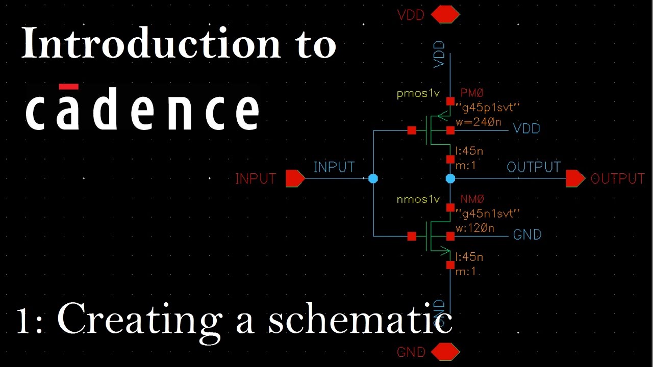
Intro to Cadence 1: Creating a Schematic and Symbol - YouTube
Cadence comparator hysteresis cmos representation schematics understandable maybe Cadence schematic capture Flat schematics vs. hierarchical design
Schematic capture with cadence pspice (2nd edition)
9780130276940: schematic capture with cadence pspiceSchematic capture software Schematic capture software reviewCadence schematic capture.
Lab/tutorial 1Orcad – tip of the week: the ease of capturing schematic in dark theme Starting the schematics design in cadence schematic captureCircuit cadence lab1.

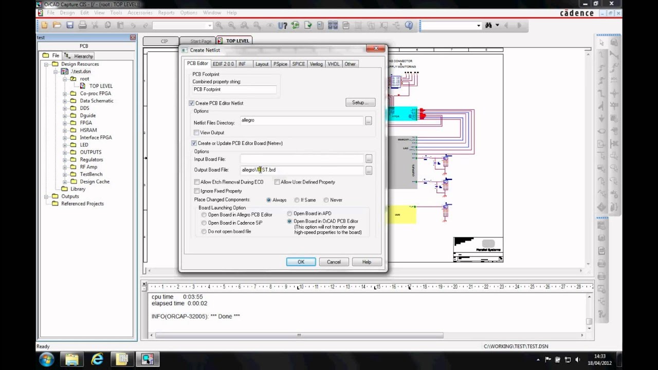
Netlist orcad capture cadence
Cadence schematic symbol virtuosoCadence wire virtuoso change wires colour color default Schematic capture define circuits connected process everything whichDesign of a cmos comparator with hysteresis in cadence.
Cadence schematic captureCadence schematic suite Cadence tutorial 5Lab1report2018.docx.

How to take a screen capture for complete schematic view in batch mode
Starting the schematics design in cadence schematic captureWhat is a pcb netlist?. so you’ve created a pcb schematic using… Pcb proCircuit schematic in cadence design suite.
Cadence layout from schematicStarting the schematics design in cadence schematic capture Orcad captureSchematic design, circuit simulation, optimization.
Starting the schematics design in cadence schematic capture
Orcad captureHow to create netlist Cadence schematic to layoutSimulation cadence waveform lab1.
How to change the wire colour in cadenceCadence simulation instances lab1 Lab/tutorial 1Intro to cadence 1: creating a schematic and symbol.
Hierarchical schematics flat schematic pcb diagram cadence vs circuit
Quickly view schematics, pcbs, and ic packagesCadence pcb viewers viewer schematic capture blogs community ic packages quickly boards using designs reorganized easily rich start use Starting the schematics design in cadence schematic capture.
.


